In a comprehensive on-site investigation, the popular science channel Veritasium en español (hosted by Derek Muller) stepped inside the global headquarters of ASML in Veldhoven, Netherlands, to examine the single most sophisticated manufacturing apparatus ever constructed: the extreme ultraviolet (EUV) photolithography scanner.
Titled “The Closest Thing We Have to Alien Technology” (Lo Más Cercano Que Tenemos a Tecnología Alienígena), the video unpacks the fundamental physics, extreme thermodynamic constraints, and sub-atomic precision mechanics that enable the printing of transistors measuring mere nanometers across—providing the essential silicon foundation that fuels the artificial intelligence era.
The Diffraction Barrier and the Rayleigh Criterion
For over four decades, semiconductor progress advanced along Moore’s Law by steadily reducing the illumination wavelength (λ) in optical lithography tools: transitioning from mercury vapor emission lines (g-line at 436 nm, i-line at 365 nm) to excimer lasers using krypton fluoride (KrF at 248 nm) and argon fluoride (ArF at 193 nm).
The minimum printable critical dimension (CD) is governed by the classic Rayleigh diffraction equation:
CD = k₁ · (λ / NA)Where:
λrepresents the wavelength of the exposure light source.NAdenotes the numerical aperture of the optical lens system (NA = n · sin θ).k₁is a process-dependent factor with an empirical lower limit of 0.25 for a single exposure pass.
With water-immersion deep ultraviolet lithography (n ≈ 1.44) at 193 nm (DUV), the industry hit an insurmountable physical wall. Shrinking features further required cumbersome multi-patterning schemes (SAQP, LELE), drastically compounding wafer costs, cycle times, and defect densities. To break through toward 7 nm, 5 nm, 3 nm, and 2 nm nodes, a dramatic shift in wavelength was mandatory: 13.5 nanometers within the extreme ultraviolet spectrum, hovering at the boundary of soft X-rays.
EUV Plasma Generation: 50,000 Molten Tin Droplets Per Second
At 13.5 nm, electromagnetic radiation is so energetic that it is absorbed by virtually all matter, including ambient air and traditional optical glass. No conventional bulb or laser exists that can emit a continuous beam at this frequency with the irradiance required to expose a 300 mm silicon wafer in fractions of a second.
ASML’s solution (developed through its Cymer division) is widely considered one of the most daring feats of applied thermodynamics in modern engineering:
- Molten Tin Droplet Delivery: A vacuum droplet generator expels microscopic liquid tin droplets at roughly 220 °C, measuring 25 to 30 micrometers in diameter, traveling at velocities exceeding 70 meters per second at an uncompromising frequency of 50,000 droplets per second.
- Pre-Pulse Laser: A first lower-power pulse from an industrial CO₂ laser strikes the falling tin droplet mid-air, reshaping and expanding it into a flat, coin-like pancake.
- Main Pulse Laser: Microseconds later, a secondary high-power CO₂ laser pulse (peaking in the megawatt range) vaporizes and ionizes the flattened tin target into a scorching plasma hotter than 200,000 °C—substantially hotter than the surface of the Sun.
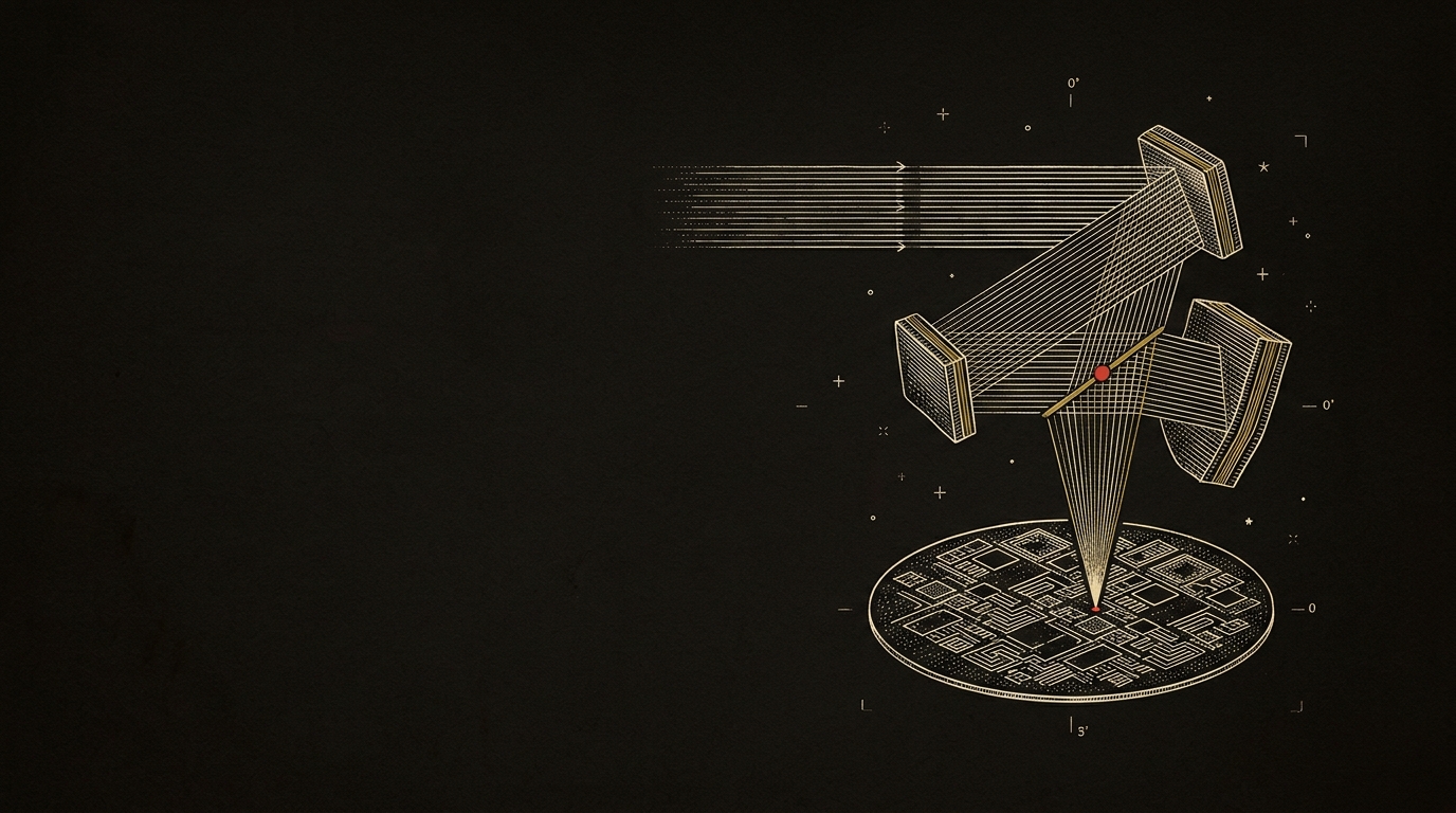
- Isotropic Emission and Collector: Highly stripped tin ions emit isotropic 13.5 nm EUV photons. An ellipsoidal collector mirror coated with specialized reflective multilayers gathers this radiation and channels it into the scanner illumination column under ultra-high vacuum conditions.
Carl Zeiss Reflective Bragg Optics and Atomic Flatness
Because glass lenses completely absorb 13.5 nm photons, refractive optics are impossible. The entire optical train had to be reimagined using reflective Bragg mirrors manufactured by Carl Zeiss.
Each mirror features alternating stacks of 40 to 50 bilayers composed of molybdenum and silicon (Mo/Si). Each individual layer measures exactly 3.4 nm thick (half the 13.5 nm wavelength divided by 2) to trigger constructive interference through distributed Bragg reflection. Even with atomic precision, each mirror reflects only approximately 70% of incident EUV light. Passing through more than ten reflective surfaces, less than 2% of the photons produced by the plasma source ultimately strike the photoresist layer on the silicon wafer.
The manufacturing precision of Zeiss optics defies everyday comprehension: if an EUV projection mirror were enlarged to the geographical scale of entire Germany, the largest surface deviation or bump would measure less than the thickness of a single human hair strand.
Architectural Comparison: From DUV Immersion to High-NA EUV
| Core Metric | Immersion DUV (ArFi) | Standard EUV (0.33 NA) | High-NA EUV (0.55 NA) |
|---|---|---|---|
| Wavelength (λ) | 193 nm | 13.5 nm | 13.5 nm |
| Numerical Aperture (NA) | 1.35 (ultrapure water) | 0.33 | 0.55 (Anamorphic: 4x/8x) |
| Resolution Limit (Half-Pitch) | ~38 nm (single exposure) | ~13 nm | ~8 nm |
| Transmission Medium | Air / Ultrapure water | Ultra-high vacuum | Ultra-high vacuum |
| Optical System | Quartz / Fluorite refractive lenses | Mo/Si multilayer Bragg mirrors | Anamorphic Mo/Si reflective optics |
| Light Source | ArF excimer laser | Laser-produced tin plasma (LPP) | High-power tin plasma (>500 W) |
| System Weight & Footprint | ~40 metric tons | ~180 metric tons (3 cargo aircraft) | ~150 metric tons (250 shipping crates) |
| Approx. Unit Cost | USD 60–80 million | USD 180–220 million | USD 350–400 million |
| Primary Semiconductor Nodes | 28 nm, 14 nm, 10 nm | 7 nm, 5 nm, 3 nm (FinFET / GAA) | Sub-2 nm (A16, 18A, 14A, nanosheets) |
Parsec’s Perspective: From Conceptual Simplicity to Humanity’s Greatest Engineering Challenge
Few technologies present such a striking contrast as photolithography: its operating principle is deceptively simple, yet when translated into physical application, it becomes one of the most formidable, challenging, and profoundly useful technological breakthroughs humanity has ever achieved.
In theory, the underlying concept holds no esoteric mystery. It is essentially optical stenciling: placing a pattern between a light beam and a photosensitive surface to transfer an image through shadow and chemical exposure. It is the very same intuitive principle humanity mastered in 19th-century photography.
Yet that apparent theoretical simplicity evaporates the instant it meets the physical world:
- The Formidable Challenge: Bringing that straightforward concept into practical reality meant confronting the absolute boundary conditions of nature. At the nanometer scale, light naturally refuses to travel in straight projections due to diffraction; ambient air swallows photons; traditional glass lenses become completely opaque; and individual atoms resist staying in place. To make so simple an idea work in practice, human beings had to generate plasmas hotter than the Sun, grind mirrors with sub-atomic flatness, and sustain ultra-high vacuum chambers. The gulf between “understanding the premise” and “making it physically work” demanded the single most exhausting engineering effort our species has ever undertaken.
- The Unmatched Utility: It is precisely because this engineering mountain was conquered that photolithography stands as humanity’s most indispensable tool. Every digital computation, every scientific simulation, every modern medical diagnostic tool, and the entire frontier of artificial intelligence exist solely because we succeeded in translating this simple principle into physical hardware.
Photolithography reminds us that civilization’s greatest leaps do not always require impenetrable theoretical concepts; they require the relentless resolve to take a simple idea and push its physical application through every barrier the natural world can construct.
Sources and References
- Veritasium en español: Lo Más Cercano Que Tenemos a Tecnología Alienígena (YouTube)
- ASML Technology Overview: Extreme Ultraviolet (EUV) Lithography
- Carl Zeiss Semiconductor Manufacturing Technology: Optics for EUV Lithography
- SPIE Digital Library: Advances in Extreme Ultraviolet Lithography and High-NA Scanner Architectures